Nanoimaging: new method paves the way for innovative materials
An international research team, including PLUS researchers, has used X-ray nanotomography to discover how tiny, self-organised structures work together. This nanoimaging technique could help to produce materials for lighting and electronics applications that have a uniform and improved structure over long distances.
Complex structures in tiny diamond networks
Using a new imaging technique, the researchers have discovered complex structures in tiny diamond networks that arise through self-organisation. This principle is similar to that in biological systems and could enable pioneering applications in materials science as it is energy and resource efficient.
To capitalise on these advantages, we need to gain a better understanding of how these structures and their irregularities – also known as defects – are created. Defects occur on different scales and can significantly affect the properties of materials. Small defects are often only 10-100 nanometres in size, but larger ones can have an effect over greater distances. Studying these defects requires techniques that can provide very precise images of these structures and analyse the large amounts of data generated.
International team makes great progress
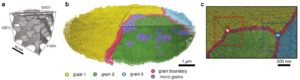
An international team, including researchers from the Department of Chemistry and Physics of Materials at the Paris Lodron University of Salzburg (PLUS), has achieved this major advance in nanotechnology. The researchers mapped the complex 3D structures in tiny diamond networks, which were synthesised and then replicated in gold. They used the advanced technique of Swiss Light Source (SLS) X-ray nanotomography to study these structures with an extremely high accuracy of 11 nanometres. This enabled them to analyse a large volume of 90 cubic micrometres and capture almost 70,000 individual units of the diamond structure.
Thanks to this technique, they were able to recognise not only individual defects, but also complex structures such as “comet” and “trefoil” patterns that occur at the boundaries of these structures. These patterns are similar to those in soft materials such as liquid crystals, but show the behaviour of hard crystals.

New materials thanks to ‘topological defects’
The researchers developed a new method for analysing tensions in the structures, inspired by the moiré effect1. They discovered that so-called ‘topological defects’ help to maintain order throughout the network. They do this by attracting and synchronising smaller defects. These findings could help to produce new materials with improved properties.
Nanoimaging has significantly improved the materials science community’s understanding of complex structures created by self-organising processes and could pave a ground-breaking way for new materials with unique properties. A study on this was recently published in Nature Nanotechnology.
1 The moiré effect is a visual phenomenon that occurs when two overlapping patterns with fine structures are slightly shifted or rotated against each other. This creates new, usually large-scale patterns known as moiré.